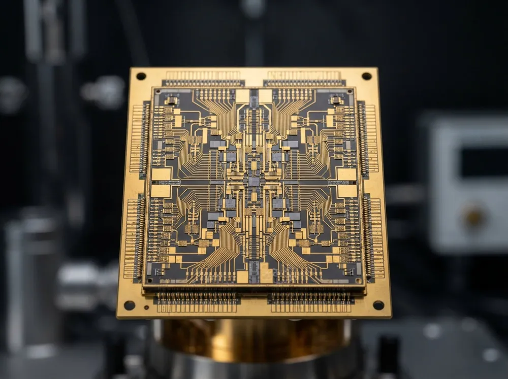
Taiwan Semiconductor Manufacturing Co. is reportedly considering producing advanced memory chips as Nvidia seeks additional supply for artificial intelligence hardware. The potential TSMC 3D DRAM initiative would expand the Taiwanese chipmaker’s role beyond its established business of manufacturing logic processors for other companies.
According to a November 6, 2026, report by The Information, TSMC has begun exploring plans to manufacture three-dimensional dynamic random-access memory at Nvidia’s request. The report cited two people with direct knowledge of the discussions. However, no production agreement, investment commitment or launch timetable has been announced.
TSMC 3D DRAM Plans Could Expand Its Role in AI Hardware
TSMC is best known for manufacturing advanced processors designed by companies including Nvidia, Apple and AMD. Moving into DRAM production would represent a significant expansion into a market dominated by Samsung Electronics, SK Hynix and Micron Technology.
The reported discussions come as memory availability becomes an increasingly important constraint on AI infrastructure development. Large AI accelerators require substantial memory capacity and bandwidth to process model parameters and intermediate calculations. Demand from data centers has also increased competition for manufacturing resources across the semiconductor industry.
The Information reported that TSMC could build dedicated manufacturing facilities or acquire an existing factory and convert it for memory production. Neither approach has been confirmed as a final decision. The company has not disclosed how much investment such a project would require.
TSMC told The Information that it does not comment on market rumors or speculation. The company also reiterated its focus on its core dedicated integrated-circuit foundry business. Nvidia did not respond to the publication’s request for comment.
How 3D DRAM Technology Works
Dynamic random-access memory temporarily stores the information processors need during active computing tasks. Conventional DRAM generally arranges memory cells across a two-dimensional structure. Three-dimensional DRAM designs instead seek to organize memory cells vertically, potentially increasing storage density without requiring proportionally larger chip surfaces.
This approach could help manufacturers overcome some physical limitations of traditional memory scaling. Packing additional storage into a smaller area may improve capacity and support increasingly demanding computing systems. However, those benefits depend on the final architecture, manufacturing process and electrical performance.
Manufacturing vertically integrated memory structures introduces substantial engineering challenges. Additional layers require precise fabrication, reliable electrical connections and effective defect control. Heat management and production yields can also become difficult as chip structures grow more complex.
Importantly, 3D DRAM should not be confused with high-bandwidth memory, or HBM. Existing HBM products stack separate DRAM dies and connect them through advanced packaging technologies. The reported 3D DRAM initiative concerns a different approach to organizing memory cells, although both technologies address growing demands for memory performance and capacity.
Why Nvidia Needs More Advanced Memory
Nvidia’s AI accelerators depend on rapid data movement between processors and memory. When that data cannot arrive quickly enough, powerful computing units may remain underutilized. Increasing memory bandwidth and capacity is therefore essential for improving the performance of large AI systems.
Memory constraints extend beyond the chip itself. Advanced packaging, power consumption, and the movement of Information between components all influence system performance. TechAmerica.ai recently examined similar limitations in its coverage of ternary AI chip research, where reducing computational precision does not eliminate memory bottlenecks.
Additional memory manufacturers could eventually give Nvidia and other chip designers more procurement options. Greater supplier diversity may reduce dependence on established producers, although qualifying new memory technologies for commercial AI systems requires extensive testing.
Any contribution from TSMC would also depend on manufacturing scale and customer adoption. The reported project remains exploratory, so it’s premature to assume it will resolve current memory shortages or lower AI hardware prices.
TSMC Already Works With SK Hynix on HBM4
TSMC has an established connection to advanced memory development through its collaboration with SK Hynix. In April 2024, the companies announced a partnership to develop HBM4 and next-generation semiconductor packaging.
Under that arrangement, SK Hynix planned to use TSMC’s advanced manufacturing technology for the HBM4 logic base die. That component manages communication between the memory stack and other parts of the computing system. SK Hynix remained responsible for its memory technology, making the collaboration different from TSMC producing DRAM independently.
The relationship has continued to evolve. At TSMC’s 2026 technology symposium, SK Hynix outlined its vision for tighter integration between memory and logic technologies. The company discussed customized HBM and three-dimensional memory-on-logic architectures as potential directions for future AI hardware.
A separate Reuters report on October 18 described plans for Samsung to use TSMC’s 3-nanometer technology for base dies in Nvidia’s next-generation custom memory products. Those developments show how closely processor manufacturing, memory design and advanced packaging are becoming connected.
Samsung, SK Hynix and Micron Face a Potential Competitor
Samsung, SK Hynix and Micron have decades of experience producing DRAM at commercial scale. Their established manufacturing processes, technical expertise and customer relationships create significant barriers for new entrants. All three are also pursuing more advanced memory technologies.
TSMC brings extensive semiconductor manufacturing capabilities, but building a competitive DRAM operation would require specialized processes and substantial investment. Experience producing advanced logic chips does not automatically translate into economical, high-yield memory manufacturing.
The financial risks are considerable. Memory markets have historically cycled through shortages, rapid capacity expansion, and subsequent oversupply. A factory approved during a period of elevated prices may begin production after market conditions have changed.
These pressures are already affecting other technology markets. TechAmerica.ai has reported on AI-driven memory demand and its implications for smartphone manufacturers as data centers compete for semiconductor supply.
What Happens Next for TSMC and Nvidia?
The immediate question is whether TSMC will convert its reported preliminary planning into a formal manufacturing program. A confirmed investment decision, factory location, production schedule or customer agreement would provide stronger evidence that the company intends to enter the advanced DRAM market.
Technical feasibility remains another uncertainty. Developing a workable 3D DRAM architecture is different from manufacturing large quantities with acceptable yields and consistent reliability. Even after production begins, manufacturers must qualify chips before deploying them in demanding commercial systems.
For Nvidia, the potential benefit is a broader long-term memory supply base. For established DRAM manufacturers, a successful TSMC expansion could introduce another major competitor. Neither outcome is assured while the project remains under consideration.
The November 6 report highlights how AI infrastructure demand is encouraging chipmakers to reconsider traditional boundaries between processors, memory and packaging. Whether TSMC ultimately enters 3D DRAM production will depend on technical progress, manufacturing economics and the durability of customer demand.