


ASML: The Machine That Saved Moore’s Law and Powers the Modern Chip Industry
ASML builds the EUV machines that power the world’s most advanced chips, enabling AI, smartphones, and high-performance computing at the limits of physics.
When people talk about the most powerful technology companies in the world, they usually mention chip designers or consumer brands. But behind every advanced processor, GPU, and AI accelerator sits one company that made it all possible: ASML.
ASML is the company that saved Moore’s Law, enabled modern AI, and reshaped the global semiconductor industry — all while remaining largely invisible to the public. This article takes a deep, step-by-step look inside ASML, explaining how microchips are made, why extreme ultraviolet lithography matters, how nuclear fusion concepts play a role, and why ASML may be the most crucial tech company in the world.
The Machine That Saved Moore’s Law
For decades, Moore’s Law predicted that the number of transistors on a chip would double roughly every two years. By the early 2000s, the industry was approaching a wall. Traditional lithography methods using deep ultraviolet (DUV) light could no longer etch transistors small enough to keep pace.
This is where ASML changed everything.
ASML developed extreme ultraviolet (EUV) lithography, a technology so complex and expensive that many believed it was impossible to commercialise. Without EUV, today’s 5nm and 3nm chips, and future 2nm chips, would not exist. Moore’s Law didn’t die — a single machine rescued it.
How Microchips Are Made (Simplified)
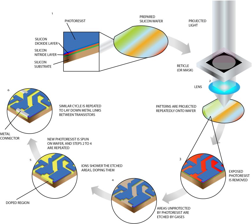
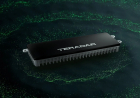
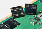
Microchip manufacturing begins with a pure silicon wafer. Layers of materials are added, etched, and patterned billions of times to create microscopic transistors.
The key step is lithography, where light is projected through a mask to print patterns onto the wafer. Each new generation of chips requires smaller, more precise patterns — and eventually, conventional light wasn’t enough.
That limitation led directly to EUV.
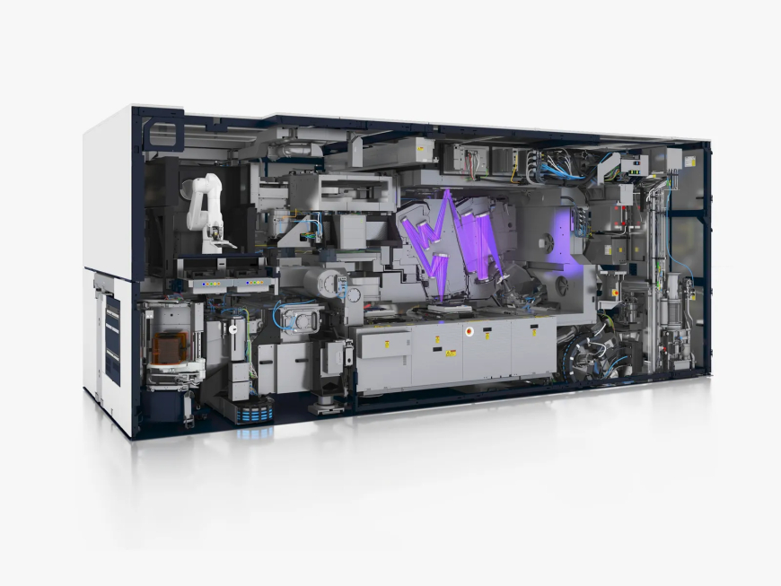
What Is Extreme Ultraviolet Lithography?
EUV lithography uses light with a wavelength of 13.5 nanometers, far smaller than previous technologies. Producing this light is one of the most complex engineering feats in human history.
There are no lenses. EUV light is absorbed by air and glass, so everything happens in a vacuum using ultra-precise mirrors. Even a single dust particle can destroy accuracy.
An EUV machine:
- Weighs over 180 tons
- Contains more than 100,000 components
- Costs over $150 million per unit
- Requires atomic-level precision
Only ASML has successfully scaled EUV.
Nuclear Fusion… in a Chip Factory
One of the most astonishing aspects of ASML’s EUV technology is how the light itself is generated.
Tiny droplets of molten tin are fired at 50,000 times per second. Each droplet is struck by a high-powered laser twice, creating a plasma hotter than the surface of the sun. This plasma emits extreme ultraviolet light, which is then reflected and shaped to print chip patterns.
The physics involved is closer to nuclear fusion research than traditional manufacturing — and it runs 24/7 inside semiconductor fabs around the world.
How ASML Conquered the Chip World
ASML didn’t dominate overnight. The company spent decades refining lithography tools while competitors abandoned EUV as too risky and expensive.
ASML succeeded because of:
- Long-term investment without short-term profits
- Deep partnerships with chipmakers
- Collaboration with hundreds of suppliers
- Unmatched engineering persistence
Today, ASML has no real competitor in EUV lithography. If you want to make advanced chips, there is no alternative.
Who Are ASML’s Biggest Customers?
ASML’s customers are the giants of the semiconductor world:
- TSMC – the world’s leading chip manufacturer
- Intel – rebuilding its manufacturing leadership
- Samsung Electronics – a significant memory and logic producer
Every advanced processor from Apple, NVIDIA, AMD, and Qualcomm depends on ASML machines — even if those companies never touch ASML directly.
The Most Important Tech Company in the World
ASML doesn’t design chips. It doesn’t sell consumer products. Yet without ASML:
- AI acceleration would stall
- Smartphone progress would slow
- High-performance computing would regress
- Moore’s Law would effectively end
ASML sits at the foundation of modern computing. Its technology determines what is physically possible in silicon.
Inside ASML: Culture, Scale, and Control
ASML operates with extreme secrecy and precision. Machines are assembled in modules across multiple countries, shipped in parts, and reassembled in fabs by specialised teams.
Each EUV system requires:
- Months to install
- Continuous calibration
- Dedicated ASML engineers on-site
This tight integration makes ASML not just a supplier, but a permanent partner in chip manufacturing.
Why ASML Will Shape the Future of Technology
As the world moves toward:
- Artificial intelligence
- Autonomous systems
- Advanced defence technology
- Quantum-adjacent computing
The need for more minor, faster, more efficient chips will only grow. ASML’s roadmap extends well beyond current EUV into High-NA EUV, pushing transistor scaling even further.
ASML isn’t just enabling the future — it’s defining its limits.
Final Thoughts
ASML is not famous, flashy, or consumer-facing — but it may be the most powerful technology company on Earth. By solving problems at the edge of physics, ASML made modern computing possible and kept Moore’s Law alive when it seemed doomed.
If you want to understand how the digital world truly works, you don’t start with chips.
You start with ASML.
What's Your Reaction?
 Like
0
Like
0
 Dislike
0
Dislike
0
 Love
0
Love
0
 Funny
0
Funny
0
 Angry
0
Angry
0
 Sad
0
Sad
0
 Wow
0
Wow
0